Introduction
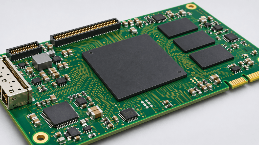
Field-Programmable Gate Arrays (FPGAs) have become the computational backbone of modern high-performance electronics. From industrial automation and medical imaging to automotive ADAS, IoT edge computing, and renewable energy systems, FPGAs deliver unmatched parallel processing power and hardware reconfigurability.
However, turning a complex FPGA architecture into a reliable physical product presents significant manufacturing hurdles. High pin-count packages, ultra-fast signal speeds, and strict thermal requirements demand a manufacturing partner with proven expertise in both High-Speed PCB Fabrication and Precision PCBA.
Key Manufacturing Challenges in FPGA Designs
Unlike standard microcontroller boards, FPGA-based hardware pushes the boundaries of conventional manufacturing:
- Signal Integrity & Impedance Control: High-speed transceivers and DDR memory interfaces require tight impedance tolerances and low-loss dielectric materials to prevent signal attenuation and crosstalk.
- High-Density Interconnects (HDI) & Layer Counts: Routing hundreds of I/O pins from fine-pitch BGA packages often necessitates high-layer-count stack-ups, blind/buried vias, and via-in-pad (VIPPO) technology.
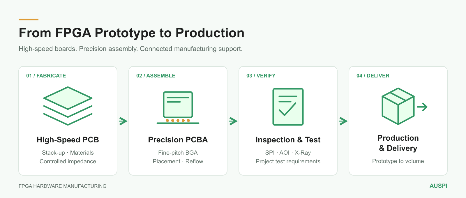
- Zero-Defect BGA Assembly: FPGA chips are high-value components. Soldering fine-pitch BGAs requires strict moisture control, precise solder paste deposition, optimized reflow profiles, and 100% X-Ray inspection to eliminate voiding or cold joints.
How AUSPI Delivers Reliable FPGA Hardware Solutions
Founded in 2003, AUSPI Enterprises integrates over two decades of EMS expertise to support your FPGA projects from initial prototype to global mass production.
1. Advanced Bare PCB Capabilities for High-Speed Signals
Our High-Speed & High-Frequency PCB manufacturing lines are engineered to maintain signal integrity across complex FPGA layouts:
- Multilayer & HDI Expertise: High-layer-count rigid and rigid-flex boards featuring microvias, blind/buried vias, and resin-plugged via-in-pad structures.
- Strict Process & Control Points: Precision controlled impedance and specialized high-frequency laminates tailored for high-speed data transmission.
2. Precision PCBA & High-Value Component Care
We treat every FPGA assembly with rigorous quality control to protect your high-value silicon:
- Fine-Pitch BGA Placement & Inspection: High-accuracy SMT lines equipped with SPI, AOI, and automated X-Ray inspection to verify hidden BGA solder joints.
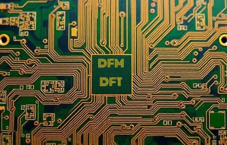
- Strict DFM & DFT Reviews: Before production begins, our engineering team conducts thorough Design for Manufacturability (DFM) and Design for Testability (DFT) checks to identify potential routing or assembly risks early.
3. Agile NPI / Prototyping with Zero MOQ
FPGA hardware often undergoes multiple design iterations before final lock-in. AUSPI removes bottlenecks from your R&D cycle:
- Rapid Turnaround: 72-hour bare PCB sampling and 2–3 weeks Turnkey PCBA prototyping.
- Total Flexibility: No Minimum Order Quantity (MOQ) requirements, allowing you to validate small batches cost-effectively.
- Turnkey Supply Chain Management: Transparent BoM cost breakdowns, live stock data, and reliable sourcing for critical FPGA chips, power management ICs (PMICs), and peripheral components.
4. Multi-Shore Global Manufacturing Security
With 4 manufacturing bases (China, Czech Republic, Mexico, Malaysia) and 8 global branches, AUSPI delivers flexible onshore, nearshore, and offshore production tailored to your supply chain needs.
Consultation and Content Support
For complete Chinese and English FPGA hardware solution content, publishing and layout recommendations, or customized social media promotional content, contact the AUSPI team or visit the official AUSPI Enterprises website for further technical and business support.