What is PCBA?
A printed circuit board (PCB) is a small green chip covered in lines and copper parts that you’ll find at the heart of gutted electronic devices. They are an integral part of our daily lives, and can be found in everything from our smartphones to our cars. At the heart of these electronics is the printed circuit board, also known as a PCB. PCBA is short for Printed Circuit Board Assembly, Generally speaking, most electronic device developing companies outsourcing a contract electronics manufacturer to do OEM assembly for their device.
What is a PCBA contract electronic manufacturer?
PCBA contract electronic manufacturer(PCB Assembly)/contract manufacturer is not an original equipment manufacturer, but a factory providing OEM electronics assembly or we can say custom electronics assembly, from components sourcing, PCB manufacturing, SMT assembly, pth assembly, functional test, box build assembly a complete turn key electronic manufacturing service. Since 2003 Auspi is your one-stop PCB Assembly partner, we understand energy efficient electronics assembly or green electronics assembly is good for your key electronics assembly. Our services range not only in wireless electronics assembly, but automotive, medical, industrial, IoT etc.
PCB assembly process (PCBA Process)
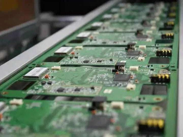
The PCB assembly process occurs after PCB manufacturing, it covers actions from stencil preparation, components/pcb baking, solder paste printing, pick and place component placement, reflow soldering, Visual inspection, AOI inspenction, X-Ray Inspection, then go to next step PTH/NPTH components placement and final inspection of the PCB functionality.
Here is a step-by-step process of PCB board assembly:
Step 1: Apply solder paste to the circuit board/PCB
The first step of PCB assembly is applying a solder paste to the PCB board. This process is like screen-printing a shirt, except instead of a mask, a thin, stainless-steel stencil is placed over the PCB.Solder paste should be applied evenly to the circuit board in the exact locations needed.
Step 2: SMD placement, or Pick and place Placement
SMDs, or surface mount components, should be placed on a prepared PCB by Pick and Place Machine.
Step 3: Refelow Soldering
In order to adhere the components to the PCB, After component placement, the board will delivery to an reflow oven, and remain in place for an extended period of time.
Step 4: Inspection
After the PCB assembly process, the operators visually inspect the PCB to check whether all parts are positioned correctly, also using AOI machine for inspection, Some board with BAG Chip, will required a special machine-X-Ray to do the solder quanlity inspection. X-Ray is An inspection used for more complex PCBs by examining the layers of the PCB and identifying potential problems.
Step 5: PTH/NPTH Component Soldering.
A plated through-hole, or PTH, component is a hole in the PCB that is plated through the holeson the board. we list a few common types of assembly method below, more informatoin, please contact us.
Manual soldering: A manual, through-hole insertion.
Wave soldering: The automated version on manual soldering where a wave of molten solders all the holes in the bottom of the board at once.
Step 6: Functional testing and final inspection
Once the soldering process of the PCB board assembly is complete, it is time to do a functonal testing if apply and final inspection.


