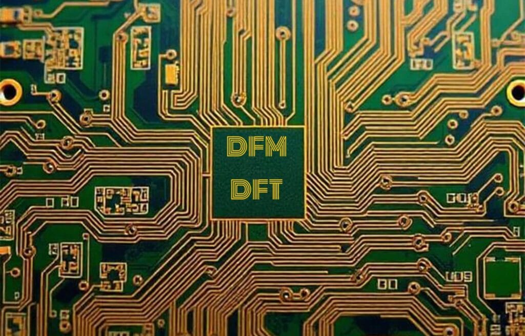
In today’s fast-moving electronics industry, designing a printed circuit board (PCB) that works well is only part of the challenge. To succeed at scale, your PCB must also be easy to manufacture and test efficiently.
This is where Design for Manufacturability (DFM) and Design for Testability (DFT) become essential. These proven approaches help reduce errors, lower costs, and speed up time to market.
Whether you’re refining a layout or managing product development, applying DFM and DFT best practices can turn complex PCB projects into streamlined, high-quality outcomes.
What is DFM in PCB Design?
Design for Manufacturability focuses on creating PCB layouts that align with real-world production capabilities. By addressing DFM early in the design stage, you avoid many common issues that cause defects, delays, and unexpected expenses.
Key DFM practices include:
- Smart component spacing – Leave enough room between parts to prevent soldering problems and improve placement accuracy.
- Standardized materials and components – Use commonly available parts to shorten lead times and control costs.
- Design for automated assembly – Optimize layouts for pick-and-place and reflow processes, favoring surface-mount technology (SMT) where possible to increase throughput.
Implementing these DFM guidelines improves PCB reliability and makes high-volume production smoother and more predictable.
How DFT Improves PCB Testing
Design for Testability ensures your PCB can be validated quickly and thoroughly during manufacturing and beyond.
In a quality-driven market, DFT helps catch faults early and supports consistent performance across production runs.
Effective DFT features to include:
- Accessible test points – Add dedicated pads for probe contact to simplify in-circuit testing (ICT).
- Well-planned signal routing – Route traces to allow easy access for testing without affecting board functionality.
- Support for multiple test methods – Design with ICT, functional testing, or boundary scan in mind to enable comprehensive inspection.
With DFT built in, your team can perform faster diagnostics and maintain tighter quality control.
Why DFM and DFT Matter for Your Bottom Line
Adopting DFM and DFT is more than a checklist item—it’s a strategic advantage. Here’s how these practices deliver value:
- Fewer manufacturing defects – Proactively designing for production reduces rework and scrap.
- Lower total cost – Efficient layouts shorten cycle times and minimize material waste.
- Faster debugging and quality assurance – Built-in testability speeds up fault identification, allowing quicker design iterations and faster market entry.
Data shows that PCBs designed with DFM and DFT principles can achieve first-pass yield rates of 90% or higher, making them critical in competitive sectors like automotive, consumer electronics, and IoT.
How AUSPI Implements DFM and DFT for Your Projects
At AUSPI, we work as an extension of your team, integrating DFM and DFT thinking from the earliest design phase. Our engineering group partners with you to provide real-time feedback, pre-production reviews, and manufacturability insights tailored to your goals.
This collaborative approach delivers:
- Higher first-pass yields (FPY) through rigorous layout analysis.
- Customized design recommendations that match your performance and volume needs.
- Smooth scaling from prototype to full production.
With AUSPI’s support, companies across industries have transformed complex PCB challenges into reliable, manufacturable solutions.